

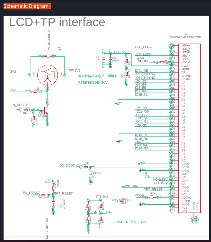
Pin mapping understanding

Refer the schematic image and main code example from the below link.
https://www.elecrow.com/wiki/esp32-display-502727-intelligent-touch-screen-wi-fi26ble-800480-hmi-display.html#schematic-pcb
facing difficulties to understand the pin mapping between that schematic and main code. Could you please share the PDF version of the schematic document?

Comments
Hi @Anand ,
The zip file contains a PDF version of the schematic diagram. And please refer to this post: https://forum.elecrow.com/index.php?p=/discussion/comment/699#Comment_699
Got it. Thank you for the clarification")
Thanks,
I was looking for an explaination for this , thanks to you I got it.You owe me my friend. Thanks once again.